Control Circuits
TODO
Key Concepts |
|
Terms
| Term | Meaning |
|---|---|
| Arithmetic Function/Circuit | Operation that processes input signals into a mathematical output. i.e. ADD, SUBTRACT. |
| Circuit | Group of transistors that implement logic, control, or storage capability in hardware. AKA Gate. |
| Digital Circuit | A circuit that operates on discrete binary (1/0) signals rather than continuous analog values. |
| Hardware Abstraction | Representing hardware as simplified layers, where each layer hides the complexity of the one beneath it. |
| Input/Output | Electrical or binary signals sent into or received out of a transistor, circuit, or arithmetic function. |
| Invert/Inversion | Switching a value/state to its opposite reference value/state. i.e. binary 1 is inverted into a binary 0. |
| Logic Function/Circuit | Operation that processes input signals into a boolean output. i.e. AND, OR, NOT. |
| Logic Gate | A circuit that implements a single boolean logic operation. i.e. AND, OR, NOT. |
| N-Type Transistor | Transistor that outputs the same reference/boolean value as its input. |
| P-Type Transistor | Transistor that outputs the opposite reference/boolean value than its input. |
| Ripple circuit | A set of identical circuits chained together to cause an output from one circuit feeds the next circuit, and affects the next circuit's result. Common in arithmetic circuits that require carry/borrow interactions between values. |
| Storage Function/Circuit | Operation that retains input signal (single bit) between clock cycles. i.e. STORE, RETRIEVE. |
| Transistors | Electronic devices used to represent binary 1 or 0 in hardware. |
| Truth Table | A tabular representation of a circuit's inputs and outputs. |
Introduction to Control Circuits
Control or Combination circuits are used to manage the flow of information from clock cycle to clock cycle. These groups of Basic Logic Circuits (opens in a new tab) consist of input/control bits, and one or more output bits.
Control circuits are used to execute the current program instruction (assembly instructions in this course). In the course of executing a single assembly instruction, the CPU's Control Unit will use required control circuits to complete actions like retrieved data, store data, add bit, read keyboard input.
The Control Unit knows what control circuits are available, how to use them, and when to use them to execute a program instruction. More on that when we talk about the Von Neumann Model in the next section.
Stateless Circuits
Circuits are sent input signals during a single clock cycle. The electrons propagate through the circuit (all the transistors in each part of the circuit) during the same clock cycle. And, within that same clock cycle, the resulting output(s) pass on to another part of the system.
Next time the same control circuit is used, it is reset. It does not remember its last results to use in producing then next result. This stateless property of control circuits. They functions control circuits provide are all simple, stand alone actions.
Download the Logisim Examples collection to examine in Logisim Circuit Simulation Tool
Decoder
Decoding is a function that converts encoded info back to its original form. The original encoding might be to make information compact (like compressing a file), converting to a different try of data (such as Digital to Analog), or using bit patterns to indicate CPU operations
We'll use the last example to talk about decoders using an over-simplified CPU.
The CPU includes the Arithmetic Log Unit (ALU). This device can perform basic math and logic operations. When the Control Unit is executing an assembly instruction, part of the instruction includes an encoded pair of bits that indicates the correct math function to execute.
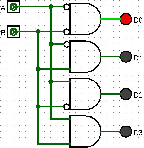
Decoder: Truth Table
| A | B | D0 | D1 | D2 | D3 |
|---|---|---|---|---|---|
| 0 | 0 | 1 | 0 | 0 | 0 |
| 0 | 1 | 0 | 1 | 0 | 0 |
| 1 | 0 | 0 | 0 | 1 | 0 |
| 1 | 1 | 0 | 0 | 0 | 1 |
A and B inputs are effectively selected 1 of the 4 outputs to be active (high). The other 3 outputs will always be inactive/low. The outputs are mutually exclusive...one (1) and only one will be active based on the inputs.
With this two (2) input Decoder, there will always be 4 outputs. In order to retain the mutually exclusive state, the input/output relationship is n inputs -> 2n outputs .
There must always be 2number of inputs outputs.
Decoder: Detailed Circuit Diagram
The decoder circuit is useful to convert encoded data to the original value. Setting A and B inputs will result in a one (1) output on 1 of the 4 lines. The example below works like a switch, with the two (2) inputs mimicking the address of the output to light up.
Decoding ISA Arithmetic Instructions
In modern ISAs, 2 bits of an instruction might represent which basic arithmetic operation to execute. In our example 16-bit ISA, bits 7 & 8 of an assembly instruction represent the math function for the Arithmetic Logic Unit (ALU)
| |Decoded Instruction|Bits 8 & 7|Operation| |-|:-:|-| |1010110**00**1111100|00|Add| |1010110**01**1111100|01|Subtract| |1010110**10**1111100|10|Multiply| |1010110**11**1111100|11|Divide| | 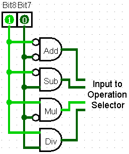 |
Bits 8 & 7 are inputs into decoder to select 1 of the 4 operations. The output of this decoder will provide input another circuit (The Operation Selector) that enables the correct arithmetic operation for the instruction.
Decoder: Simplified Component
To simplify more complicate circuit diagrams, the Decoder has a symbol that hide the inner workings.
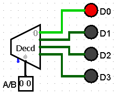
Like the circuit above this symbol has 2 inputs (A and B) and four (4) mutually exclusive outputs (D0, D1, D2, and D3).
Multiplexer
A Multiplexer chooses one (1) outputs from multiple inputs. The input value is unaltered by the circuit. It will retain its current value. The Selection signals allow 1 of the inputs through the circuit and blocks the others.
The Selection signals are set outside the multiplexer and set to cause a particular input value to be selected to be output
With 4 inputs, a multiplexer requires 2 Selection inputs. N inputs -> √2 selection signals
2n input values require n selection signals
Multiplexer: Truth Table
| S1 | S2 | ||||
|---|---|---|---|---|---|
| 0 | 0 | A | |||
| 0 | 1 | B | |||
| 1 | 0 | C | |||
| 1 | 1 | D |
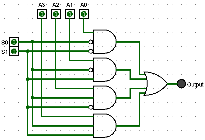
Multiplexer: Detailed Circuit Diagram
The selection signals enter each AND gate with a different set of normal and inverted modifiers
Inverted signals is effective run through a NOT gate or flipped. Normal signals unaltered
Note that S0 and S1 entering each AND gate have a different pair of normal/inverted settings. The first has both inputs inverted, the next has S0 inverted and S1 normal. The third has S0 normal and S1 inverted. The fourth has both normal
This causes the mutual exclusive behavior when selecting an input signal to output
The four (4) input values are all normal connections. Each is allowed into the its AND gate unaltered.
Multiplexing ISA Arithmetic Instructions
In modern ISAs, 2 bits of an instruction might represent which data source to use. We have 4 1-bit values from 4 memory locations. In our example 16-bit ISA, bits 2 & 1 of an assembly instruction contain an address/reference for each source.
| |Decoded Instruction|Bits 2 & 1|Operation| |-|:-:|-| |1010110001111**00**0|00|L1 Cache| |1010110011111**01**0|01|Temp Register| |1010110101111**10**0|10|RAM| |1010110111111**11**0|11|Keyboard| | 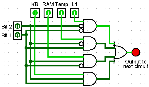 |
Each of the 4 source devices is sending a 1 into the multiplexer. Bits 2 & 1 from the instruction are used to select one (1) of the four (4) sources to pass on to the next circuit using the value.
Multiplexer: Simplified Component
We can use the simpler multiplexer symbol keep our diagram clean
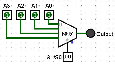
Input value and selection signals work the same as above
Conclusion
Control circuits do not retain their state between clock cycles. In each cycles control circuits reset to a neutral state and react to the new set of inputs.
Decoder circuits use input bits to select one and only one output. These devices effectively select one form several options
Multiplexer (Mux) circuits are used to pick one of several external signals to allow through this circuit.