Storage Circuits
TODO
Key Concepts |
|
Terms
| Term | Meaning |
|---|---|
| Arithmetic Function/Circuit | Operation that processes input signals into a mathematical output. i.e. ADD, SUBTRACT. |
| Circuit | Group of transistors that implement logic, control, or storage capability in hardware. AKA Gate. |
| Digital Circuit | A circuit that operates on discrete binary (1/0) signals rather than continuous analog values. |
| Hardware Abstraction | Representing hardware as simplified layers, where each layer hides the complexity of the one beneath it. |
| Input/Output | Electrical or binary signals sent into or received out of a transistor, circuit, or arithmetic function. |
| Invert/Inversion | Switching a value/state to its opposite reference value/state. i.e. binary 1 is inverted into a binary 0. |
| Logic Function/Circuit | Operation that processes input signals into a boolean output. i.e. AND, OR, NOT. |
| Logic Gate | A circuit that implements a single boolean logic operation. i.e. AND, OR, NOT. |
| N-Type Transistor | Transistor that outputs the same reference/boolean value as its input. |
| P-Type Transistor | Transistor that outputs the opposite reference/boolean value than its input. |
| Ripple circuit | A set of identical circuits chained together to cause an output from one circuit feeds the next circuit, and affects the next circuit's result. Common in arithmetic circuits that require carry/borrow interactions between values. |
| Storage Function/Circuit | Operation that retains input signal (single bit) between clock cycles. i.e. STORE, RETRIEVE. |
| Transistors | Electronic devices used to represent binary 1 or 0 in hardware. |
| Truth Table | A tabular representation of a circuit's inputs and outputs. |
Introduction to Storage Circuits
The primary function of storage circuits is to retain information between clock cycles. This is commonly called Statefulness as these circuits remember their last state for future clock cycles.
Download the Logisim Examples collection to examine in Logisim Circuit Simulation Tool
Storage Circuit vs Gate/Control Circuit Output
Gates and Control Circuits output a value based on the current input/inputs. As soon as the inputs change, the output can change. The input value causes a part of the whole circuit to produce the output. Other sections do not produce an output that influences the overall output of the circuit.
The inputs propagate quickly through the circuit and produce the output value during a single clock cycle.
Storage Circuits also propagate the output value during a single clock cycle. However, it is not a single part of the Storage Circuit that causes the output. Instead, all parts of the circuit work together to produce the output. Think of the output as a result from the circuit and not a single gate or section of the circuit.
Input Pulses
Because storage circuits hold their state, the input/inputs do not need to be maintained for the entire clock cycle. They only need to be held high or low enough to allow the value to propagate through the circuit. We will refer to this a a pulse or pulsing an input.
When examining storage circuits in Logisim, click an input to make it high, them click again to make the input low. The circuit will maintain the overall output, even after removing the high input.
Notice that, starting with the Set-Reset Latch circuit, a 1 is applied on the Set to cause the circuit to output a 1. We use 1 on the Reset to cause the circuit to output 0.
Basic Latch
Note that the simple Latch circuit, below, has the output fed back in as an input. This is a key characteristic of storage circuits, and the feature that creates statefulness.
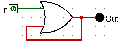
The an initial state (the state at power-up of the computer) of In is 0 . The Out is unknown.
Toggling In to 1 produces a 1 output in the OR gate. The 1 is fed back into the OR gate's 2nd input.
Toggling In back to 0 does not change the output, because the 1 fed back from the output keeps the OR gate outputting a 1.
The Flip-Flip is essentially stuck outputting a 1.
To be useful, a Latch circuit must easily switch between 0 and 1 based on the input value
Set-Reset Latch
By adding a second OR gate and cross-connecting the gates, the Set-Reset Latch overcomes the issue of getting stuck that the Basic Latch experiences.
Pulse the Set input high to make the Set-Reset Latch hold a 1
Pulse the Reset input high to make the Set-Reset Latch reset to a 0
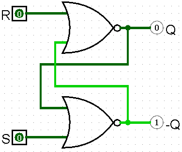
The single OR gate has been switched to a NOR gate.
Recall from NOR Gate section that there are 2 less transistors in a NOR, compared to and OR gate
The use of NOR gates is required because the output to input feedback connections do not feed back to themselves, but to the other NOR gate. The outputs are cross-connected. A Set-Reset Latch built using OR gates will still get stuck outputting 1
In the diagram, above, the top NOR gate's function is to react to the Reset input. The bottom NOR gate reacts to the Set input. Recall from the Introduction section, Set or Reset are pulsed to 1 to set the storage circuit to 1 or 0.
Truth Table
| Set | Reset | Q | -Q |
|---|---|---|---|
| 0 | 0 | 1 or 0 | 0 or 1 |
| 0 | 1 | 0 | 1 |
| 1 | 0 | 1 | 0 |
| 1 | 1 | 0 | 0 |
Initial state of Set 0 and Reset 0 is effectively an unknown state. Outputs can Q 1/-Q* 0 or vice-versa.
Set 1 and Reset 1 is a contradictory state that upstream circuits setting this Latch must prevent. This issue is a flaw in the Set-Reset Flip-Flip
Pulsing Set or Reset individually causes the circuit to hold a 1 or 0
With two (2) NOR gates, this Flip-Flip produces 2 outputs, Q and -Q. These outputs will be opposite values, typically. The circuit's output value will be from Q
Latches and Flip-Flops 1 - The SR Latch - Computer Science - UK YouTube Provider
This is the first in a series of computer science videos about latches and flip-flops..
Copyright TODO
Set-Reset Latch with Enable
The addition of two AND gates and the EN input create an Enable feature to the Set-Reset Latch. Using AND gates ensures that the Set or Reset input will only be allowed through into the core Set-Reset gates when the EN input is high. Once EN is high, the Set or Reset input behaves the same as the above circuit.
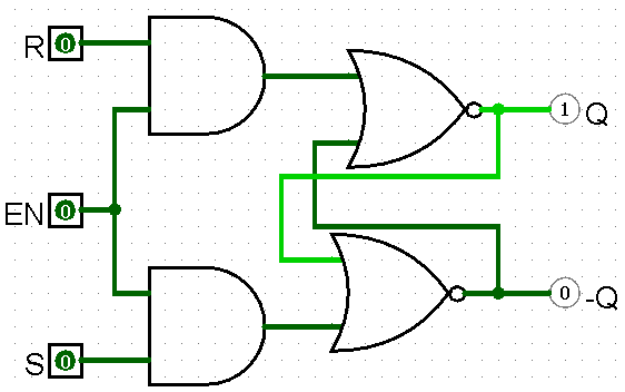
The EN input can prevent stray Set/Reset signals from updating the circuit. It also facilitates a delaying or coordinating updates within a clock cycle. Also, describes in the next section, it also facilitates a simple Memory Management construct for addressing specific circuits.
| Set | Reset | EN | Q | -Q |
|---|---|---|---|---|
| 0 | 0 | 1 | 1 or 0 | 0 or 1 |
| 0 | 1 | 1 | 0 | 1 |
| 1 | 0 | 1 | 1 | 0 |
| 1 | 1 | 1 | 0 | 0 |
| 0 | 0 | 0 | Last State | Last State |
| 0 | 1 | 0 | Last State | Last State |
| 1 | 0 | 0 | Last State | Last State |
| 1 | 1 | 0 | Last State | Last State |
Use of Write Enable with Storage
In practice, the upstream circuit is likely directly connected to many storage circuits. To facilitate this circuit changing the correct storage circuit, each storage circuit has a write-protect capability to prevent unwanted updates.
The upstream circuit will send, for example, a Set to all storage circuits it is connected to, but only the one with its Write Enable on will allow the Set into its input.
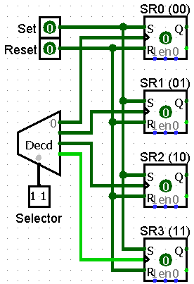
Consider the 4 Set-Reset Latches in the above diagram. They share a single pair of Set and Reset inputs. Each Set-Reset circuit is shows an a high-level symbol that hides the inner-workings.
The Decoder and Selector circuits are used to pick one of the four Set-Reset Flip-Flips to update. The Set or Reset input to then pulsed to update the selected Flip-Flip. When examining this circuit in Logisim, notice that when the Set or Reset is pulsed, all four Flip-Flips receive the pulse. The Write Enable, connected to an output of the Decoder, prevents all but the selected Flip-Flip from allowing the pulse to, updating the state of the Flip-Flip.
A negative effect of managing Flip-Flips in groups like this is that only 1 can be updated in a single clock cycle.
Latches and Flip-Flops 2 - The Gated SR Latch - Computer Science - UK YouTube Provider
This is the second in a series of computer science videos about latches and flip-flops. These bi-stable combinations of logic gates form the basis of computer memory, counters, shift registers, and more..
Copyright TODO
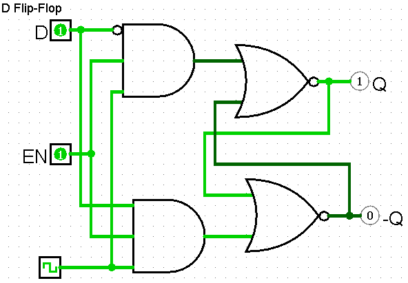
D (Data) Latch
The primary issue with the Set-Reset Latch is the possibility of both the Set and Reset inputs being active at the same time. With some slight modifications to the Set-Reset Latch with Enable, we can remove this issue.
The Set-Reset Latch was further complicated with requiring two (2) separate actions to cause the circuit to hold a 1 or a 0.
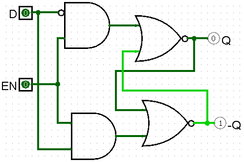
The D Latch removed the Set and Reset inputs and adds the D input. This input simply supplied the state the Latch is to hold. The D input is also pulsed like the Set-Reset circuit.
The EN input working like the enable on the Set-Reset circuit, only allowing the D input into the circuit when EN is high or enabled.
Latches and Flip-Flops 3 - The Gated D Latch - Computer Science - UK YouTube Provider
This is the third in a series of videos about latches and flip-flops. These bi-stable combinations of logic gates form the basis of computer memory, counters, shift registers, and more..
Copyright TODO
When a Latch Works as a Flip-Flop
Latch and Flip-Flop are sometimes used interchangeably, however there is one (1) primary different between them.
A Latch can update anytime the input signals and enable input are set. Even between clock-cycles
A Flip-Flop use the clock signal as an enable, so will only change when the clock pulses. Between clock pulses, inputs and other enable signals may change, however the Flip-Flip will not change state until the clock pulse occurs, letting the inputs enter the circuit
Using Propagation to Detect Clock Cycle Start
Recall that voltage takes time to propagate through each transistor in a gate or circuit. So, simplifying circuits to use less transistors will cause a gate or circuit to settle into its state earlier in the clock cycle.
And, it should make sense that adding more transistors will result in a gate to take longer to settle.
In the following circuit, consider what is happening inside the AND gate when the input is first set to high
Whats Going On Inside the AND Gate
The overall behavior of this AND Gate will be to output a 0 always. With 1 input always negated by the NOT Gate, the AND Gate will never receive 2 1 inputs needed to output a 1
With the input sending 0 into this AND gate, one input like is settled on 0 and the other (with the NOT Gate) is settled at 1 going in to the AND Gate
In the first nanoseconds after the input is it set to 1, the top input will send the 1 into the AND Gate. Because the other input had a NOT gate inline, the 1 will continue going in to the AND Gate unto the transistors in the NOT Gate settle to 0. In this short period before the NOT Gate settles, the AND Gate has 2-1 inputs and will output a 1
Quickly after the input changes, the NOT Gate will settle to 0 and the AND Gate will output 0
What this circuit does, using the delayed propagation, is to detect the Leading Edge (start) of an event. The change of an input in this example.
If, instead is connecting an input to this circuit, we connect the clock, the Leading Edge of the clock cycle is detected.
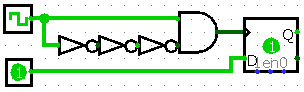
With the Leading Edge Clock Cycle circuit connected to a D Flip-Flop's Enable line, the D Flip-Flop will automatically be write enabled at the start of a clock cycle, then disabled for the remaining time of that cycle
Why 3 NOT Gates
Using more that 1 NOT Gate ensure the propagation will be long enough to pulse the write enable input
Increasing NOT Gates will lengthen the pulse. This may be needed with high-quality transistors that have low propagation times
And, NOT Gates must be in an odd-number configuration, to ensure the pulse occurs at the leading edge of the clock cycle
Conclusion
Storage 'memory' circuits retain the bit values between clock cycles. This required the controlling logic to reset these circuits if required.
There are several basic latch types that retain data.
Including write-enable circuits, a latch can be protected from unexpected update.