
Designing Circuits
TODO
Key Concepts |
|
Terms
| Term | Meaning |
|---|---|
| Arithmetic Function/Circuit | Operation that processes input signals into a mathematical output. i.e. ADD, SUBTRACT. |
| Circuit | Group of transistors that implement logic, control, or storage capability in hardware. AKA Gate. |
| Digital Circuit | A circuit that operates on discrete binary (1/0) signals rather than continuous analog values. |
| Hardware Abstraction | Representing hardware as simplified layers, where each layer hides the complexity of the one beneath it. |
| Input/Output | Electrical or binary signals sent into or received out of a transistor, circuit, or arithmetic function. |
| Invert/Inversion | Switching a value/state to its opposite reference value/state. i.e. binary 1 is inverted into a binary 0. |
| Logic Function/Circuit | Operation that processes input signals into a boolean output. i.e. AND, OR, NOT. |
| Logic Gate | A circuit that implements a single boolean logic operation. i.e. AND, OR, NOT. |
| N-Type Transistor | Transistor that outputs the same reference/boolean value as its input. |
| P-Type Transistor | Transistor that outputs the opposite reference/boolean value than its input. |
| Ripple circuit | A set of identical circuits chained together to cause an output from one circuit feeds the next circuit, and affects the next circuit's result. Common in arithmetic circuits that require carry/borrow interactions between values. |
| Storage Function/Circuit | Operation that retains input signal (single bit) between clock cycles. i.e. STORE, RETRIEVE. |
| Transistors | Electronic devices used to represent binary 1 or 0 in hardware. |
| Truth Table | A tabular representation of a circuit's inputs and outputs. |
Introduction to Designing Logic Circuits
Using Truth Tables a circuit's function is documented. The complete set of possible inputs and outputs are declared and the expected behavior is defined.
Using a 3-step algorithm, a circuit diagram can be created that implements the expected behavior.
The result will produce the expected outputs given the set of inputs. However, the circuit may contain redundant elements of unnecessary section that can be simplified.
Download the Logisim Examples collection to examine in Logisim Circuit Simulation Tool
Truth Table to Circuit Diagram
TIP
- Add an AND gate for each 1 output
- Negate each AND gate input where the value is zero (0)
- Connect Outputs of each AND gate to an OR gate
This algorithm employs boolean arithmetic's Sum of Products function.
The AND gates produce a Product of the inputs.
The OR gate sums the individual Products into the correct output value.
Simple Example
Below is a truth table for a circuit to build
| A | B | C | Zout |
|---|---|---|---|
| 0 | 0 | 0 | 0 |
| 0 | 0 | 1 | 1 |
| 0 | 1 | 0 | 0 |
| 0 | 1 | 1 | 0 |
| 1 | 0 | 0 | 0 |
| 1 | 0 | 1 | 0 |
| 1 | 1 | 0 | 1 |
| 1 | 1 | 1 | 0 |
Simple Example: Add an AND gate for each 1 output
There are 2 lines in the truth table that contain a 1 output. Lines 2 and 7. Add 2 AND gates to represent this outputs
We ignore all the zero (0) outputs as we do not need any devices to product a zero (0). Think of it as things are naturally zero (0) unless we add transistors and gates to cause a one (1) output to occur
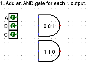
Two (2) AND gates are added to the circuit. They are all 3-input gates because the truth table contains 3 (three) inputs.
Labels were added to the Logisim elements to make the AND gates obvious.
This is also a good time in Logisim to add the three (3) inputs.
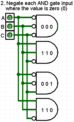
Simple Example: Negate each AND gate input where the value is zero (0)
Decide which input on each AND gate will be connected each input device. It is recommended that the top input of each AND gate receive the first input. Each lower input receive the next input on the truth table.
Examine the line on the truth table that represents the particular AND gate. If the associated input signal is zero(0), invert (NOT) the input at the AND Gate.
If the associates input signal is 1, no inversion is needed.
Because we want a 1 output from an AND gate associates with a particular line in the truth table, we must flip any zero (0) input signals to one (1) before they enter that AND gate. This is the only way to get the expected one (1) output from the AND gate.
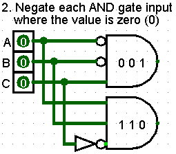
The top AND gate, associated with the truth table line 0 0 0 -> 1, has the top (A) and middle(B) inputs inverted. A and B are inverted by setting the inputs of the AND gate to NEGATE.
The bottom AND Gate, associated with the truth table line 1 1 0 -> 1, has the bottom (C) inverted. C in inverted by adding a NOT gate inline between the input device and the AND gate input connector.
In Logisim, each AND gate input can be configured with a NOT gate (the small circle symbol at the input connector). Either method works, and are the same circuit. One help make the diagram a little cleaner.
The input devices are connected to their associated input connectors on each AND gate:
- A input is connected to the Top connector of each AND gate
- B input is connected to the Middle connector of each AND gate
- C input is connected to the Bottom connector of each AND gate
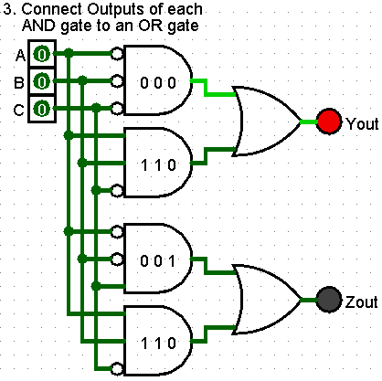
Simple Example: Connect Outputs of each AND gate to an OR gate
Add one (1) OR gate to the diagram. This gate will Sum the Product of the inputs.
The OR gate will have the same number of inputs as the number of AND gates.
Each AND gate output is connect one of the OR gate inputs.
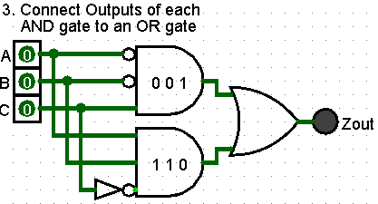
An output device is added to show the output of the OR gate
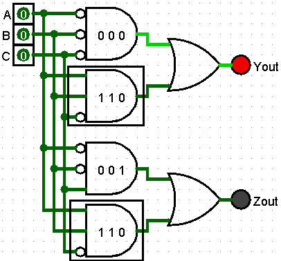
Multiple Outputs
Truth tables may have more than one (1) output for the same inputs. In this case, a circuit diagram is generated using the algorithm with all the inputs and one (1) of the outputs. It is then repeated for all inputs and the next output. This is continued until a circuit diagram is generated for all outputs
Below is a truth table for a circuit to build
| A | B | C | Yout | Zout |
|---|---|---|---|---|
| 0 | 0 | 0 | 1 | 0 |
| 0 | 0 | 1 | 0 | 1 |
| 0 | 1 | 0 | 0 | 0 |
| 0 | 1 | 1 | 0 | 0 |
| 1 | 0 | 0 | 0 | 0 |
| 1 | 0 | 1 | 0 | 0 |
| 1 | 1 | 0 | 1 | 1 |
| 1 | 1 | 1 | 0 | 0 |
Two circuit diagrams will be created. The first is for A,B,C -> Yout. The other is for A,B,C -> Zout.
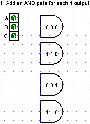
Multiple Outputs: Add an AND gate for each 1 output
The first two (2) AND gates are for the A,B,C -> Yout circuit The second two (2) AND gates are for the A,B,C -> Zout circuit (note this circuit is the same as the Simple Example)
Multiple Outputs: Negate each AND gate input where the value is zero (0)
Invert the first two (2) AND gates based on the A,B,C -> Yout part of the truth table. Invert the second two (2) AND gates based on the A,B,C -> Zout part
The A input device is connected to the first input of All AND gates. Likewise, B and C are connected to All middle and bottom inputs respectively.
Note that while we have multiple outputs, the truth table has the same 3 inputs for all outputs.
Multiple Outputs: Connect Outputs of each AND gate to an OR gate
With two (2) outputs, two (2) OR gates are added, each connected to the associated AND gates and the appropriate output device.
Optimizations
After implementing a circuit diagram from a truth table using the 3-Step Algorithm, some elements may be simplified and still produce the correct outputs.
Examining the Truth Table and the resulting Circuit can reveal redundancies and unnecessary sections that can be removed and/or recombined to simplify the circuit.
Optimization is not required. The algorithm will produce the correct circuit
However, it is cheaper and more efficient to reduce parts of a circuit. By removing gates, the final circuit will have fewer transistors needed
Redundancies
Looking at the truth table, there is a row where the same inputs result in a 1 to both outputs
| A | B | C | Yout | Zout | |
|---|---|---|---|---|---|
| 0 | 0 | 0 | 1 | 0 | |
| 0 | 0 | 1 | 0 | 1 | |
| 0 | 1 | 0 | 0 | 0 | |
| 0 | 1 | 1 | 0 | 0 | |
| 1 | 0 | 0 | 0 | 0 | |
| 1 | 0 | 1 | 0 | 0 | |
| -> | 1 | 1 | 0 | 1 | 1 |
| 1 | 1 | 1 | 0 | 0 |
Note that the 7th line of the truth table produces a 1 for both outputs when the inputs are 1, 1, 0.
Looking at the circuit diagram there are two AND gates, there are two (2) AND gates that receive 1, 1, 0 inputs.
Above the circuit diagram includes two (2) AND gates that handle the 1 1 0 inputs. They are redundant parts. These two AND gates is connected to a different outputs device
To optimize the circuit diagram
- One (1) of the duplicate AND gates is deleted
- The output of OR gate connected to the deleted AND gate is now connected to the remaining AND gate
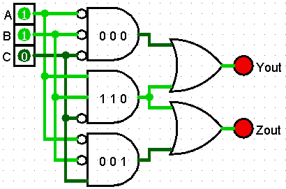
The remaining 1, 1, 0 AND Gate produces the Product for the 7th line of the truth table. The output of that AND gate it connected to both OR gates, producing the correct Sum result for each output on the truth table.
Unnecessary Sections/Ambiguities
Examining the truth table may show that an input has no actually effect on the outputs
| A | B | C | Zout | |
|---|---|---|---|---|
| 0 | 0 | 0 | 0 | |
| -> | 0 | 0 | 1 | 1 |
| 0 | 1 | 0 | 0 | |
| -> | 0 | 1 | 1 | 1 |
| -> | 1 | 0 | 0 | 1 |
| 1 | 0 | 1 | 0 | |
| -> | 1 | 1 | 0 | 1 |
| 1 | 1 | 1 | 0 |
Circuit Diagram using the 3-Step Algorithm
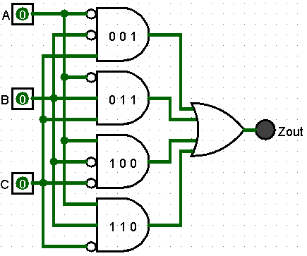
Examine the rows with a 1 output
The circuit outputs a 1 when C -> 1 and (B -> 1 or B-> 0)
The circuit outputs a 1 when A -> 1 and (B -> 1 or B-> 0)
It appears that B does not influence the output. Only A and B cause a 1 output
Remove the B input and reduce the inputs to each and gate
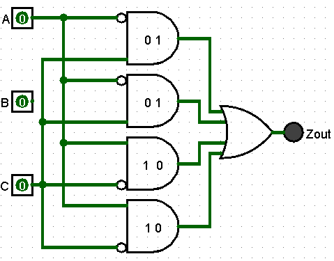
The AND gates only need 2 inputs each, so the number of transistors has been reduced, resulting in a simpler and cheaper circuit to build.
Looking at this circuit diagram, it appears there are some Redundancies that can also be further optimized to reduce the circuit's complexity and cost.
Conclusion
More complex circuits can be created from a truth table, using the 3-step algorithm. The resulting circuit will implement the truth table.
Complex circuits can be optimized, primarily by examining the Truth Table and the resulting Circuit. It may be possible to removing redundant sections in the circuit, delete unused inputs, and/or decreasing unneeded components.